How To Draw Schematic Diagrams
By Paul Horowitz and Winfield Hill
Appendix E from The Art
of Electronics 2nd Edition
Cambridge University Press
1980, 1989.

Reprinted with permission from the publisher.
My thanks to the authors for their enthusiastic support.
A well-drawn schematic makes it easy to understand how a circuit works
and aids in troubleshooting; a poor schematic only creates confusion.
By keeping a few rules and suggestions in mind, you can
draw a good schematic in no more time than it takes to draw a poor one.
In this appendix we dispense advice of three varieties: general
principles, rules, and hints. We have also drawn some real knee-slappers
to illustrate habits to avoid.
General Principles
- Schematics should be unambiguous. Therefore, pin numbers,
parts values, polarities, etc., should be clearly labeled to avoid
confusion.
- A good schematic makes circuit functions clear. Therefore,
keep functional areas distinct; don't be afraid to leave blank areas
on the page, and don't try to fill the page. There are conventional
ways to draw functional subunits; for instance, don't draw a differential
amplifier as in Figure E1, because the function won't be easily recognized.
Likewise, flip-flops are usually drawn with clock and inputs on the left,
set and clear on top and bottom, and outputs on the right.
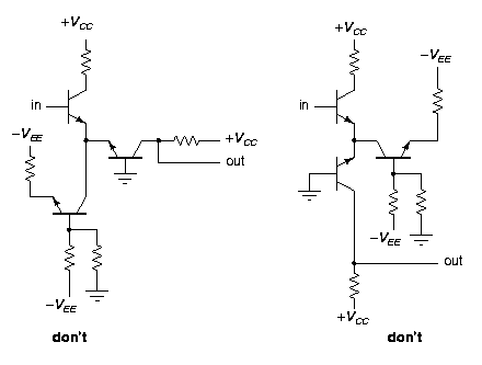
Figure E1: Placement
of power rails and conventions
for device alignment (examples of what not to
do)
Rules
- Wires connecting are indicated by a heavy black dot; wires
crossing, but not connecting, have no dot (don't use a little half-circular
``jog''; it went out in the 1950s).
- Four wires must not connect at a point; i.e., wires must not
cross and connect.
- Always use the same symbol for the same device; e.g., don't draw
flip-flops in two different ways (exception: assertion-level logic
symbols show each gate in two possible ways).
- Wires and components are aligned horizontally or vertically,
unless there's a good reason to do otherwise.
- Label pin numbers on the outside of a symbol, signal names on
the inside.
- All parts should have values or types indicated; it's best to
give all parts a label, too, e.g., R7 or IC3.
Hints
- Identify parts immediately adjacent to the symbol, forming a
distinct group giving symbol, label, and type or value.
- In general, signals go from left to right; don't be dogmatic
about this, though, if clarity is sacrificed.
- Put positive supply voltages at the top of the page, negative
at the bottom. Thus, npn transistors will usually have their
emitter at the bottom, whereas pnp's will have their emitter
topmost.
- Don't attempt to bring all wires around to the supply rails, or
to a common ground wire. Instead, use the ground symbol(s) and labels
like +Vcc to indicate those voltages where needed.
- It is helpful to label signals and functional blocks and show
waveforms; in logic diagrams it is especially important to label
signal lines, e.g., RESET' or CLK.
- It is helpful to bring leads away from components a short
distance before making connections or jogs. For example, draw
transistors as in Figure E2.
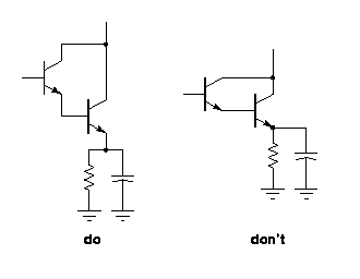
Figure E2:
Component leads
- Leave some space around circuit symbols; e.g., don't draw
components or wires too close to an op-amp symbol. This keeps the
drawing uncluttered and leaves room for labels, pin numbers, etc.
- Label all boxes that aren't obvious: comparator versus
op-amp, shift register versus counter, etc. Don't be afraid to
invent a new symbol.
- Use small rectangles, ovals, or circles to indicate card-edge
connections, connector pins, etc. Be consistent.
- The signal path through switches should be clear. Don't
force the reader to follow wires all over the page to find out how
a signal is switched.
- Power-supply connections are normally assumed for op-amps and
logic devices. However, show any unusual connections (e.g., an op-amp
run from a single supply, where V- = ground) and the disposition of
unused inputs.
- It is very helpful to include a small table of IC numbers, types,
and power-supply connections (pin numbers for Vcc and ground, for
instance).
- Include a title area near the bottom of the page, with name of
circuit, name of instrument, by whom drawn, by whom designed or checked,
date, and assembly number. Also include a revision area, with
columns for revision number, date, and subject.
- We recommend drawing schematics freehand on coarse graph paper
(nonreproducing blue, 4 to 8 lines per inch) or on plain paper on top
of graph paper. This is fast, and it gives very pleasing results.
Use dark pencil or ink; avoid ball-point pen.
As an illustration, we've drawn a humble example (Figure E3) showing
``awful'' and ``good'' schematics of the same circuit; the former
violates nearly every rule and is almost impossible to understand.
See how many bad habits you can find illustrated. We've seen all
of them in professionally drawn schematics! (Drawing the ``bad''
schematic was an occasion of great hilarity; we laughed ourselves
silly.)
Figure E3 (A):
An awful schematic

Figure E3 (B): A
good schematic

 Back to the xcircuit home page. . .
Last updated: April 4, 2006 at 5:18pm